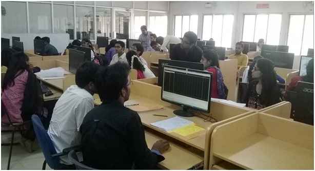
VLSI Labaratory
Analog and Digital IC Design Laboratory
This Laboratory is equipped with Cutting-Edge Technology EDA Tools such as Cadence Virtuoso Bundle Software (IC-6.1.5) for Chip Tape-out, Mentor Graphics Calibre for DRC/LVS Validation, Synopsys for Digital IC design and validation, Cadence orCAD for PCB design, Xilinx ISE for IP-core design and validation. This lab is also equipped with advanced equipment (Agilent 3GHz Spectrum Analyzer, Tektronix 1GHz oscilloscope, Agilent 200MHz DSO, 3GHz RF Signal generator, Mixed signal oscilloscope 350MHz, HP 100MHz oscilloscope, 68-channels Logic Analyzer, 7GHz Spectrum Analyzer and 6GHz Vector Signal Generator) and FPGA hardware kits (Xilinx Spartan 3-E/Vertex-5/Vertex-II Pro/ Vertex-7/ Xtreme DSP, Altera DE1/DE2 Cyclone II/ DSP Startix II/III, Xilinx Kintex-7/ Xilinx Zync/NET FPGA, FPGA with High-speed Analog modules, WARP V3 kit/ FMC RF-2X245 Dual Radio/USRP N210 Boards) which support for conducting the UG/PG labs and also research activities in M.S and PhD level
List of PG Experiments
1. MOS characteristics
2. Common Source Amplifier
3. Common Gate Amplifier
4. Common Drain Amplifier
5. Current Mirror
6. Differential Amplifier
7. Telescopic operational Amplifier
8. Folded Cascode Operational Amplifier
9. Two stage Operational Amplifier
ASIC CAD Laboratory
The lab is supported by DeitY, New Delhi
Introduction to the Laboratory
This Lab gives an idea of Pre-Layout and Post-Layout Analysis, Synthesis, Simulation, and Layout generation to the students. The lab uses Cadence and Synopsys Tools to handle the analysis. Verilog HDL is being used by the students to realize the problems as a circuit.
List of Development Boards
| SL. No |
Board Details |
Quantity |
Fund Type |
| 1 |
Xilinx Virtex 7 Development Board |
1 |
TEQIP-II |
| 2 |
Xilinx Virtex 5 Development Board |
2 |
Plan |
| 3 |
Xilinx Kintex 7 FPGA DSP kit |
2 |
SMDP |
| 4 |
Virtex II Pro Kit |
5 |
SMDP |
| 5 |
Xilinx Zync FPGA Board |
1 |
TEQIP |
| 6 |
BASYS 3 Board |
10 |
SMDP |
| 7 |
ZYBO Board |
5 |
SMPD |
| 8 |
Nexys 4 DDR |
5 |
SMDP |
| 9 |
Analog Discover Kit |
3 |
SMDP |
| 10 |
Intel Galileo Gen 2 MB |
10 |
Intel |
| 11 |
NET FPGA |
2 |
Plan |
| 12 |
DSP Stratix-III Kit |
2 |
DIT |
| 13 |
DSP Stratix-II Kit |
2 |
SMDP |
| 14 |
Xtreme DSP Kit for Virtex-4 |
2 |
SMDP |
| 15 |
Xilinx Spartan 3E Kit |
15 |
SMDP |
| 16 |
Altera DE1 Cyclone II Kit |
2 |
DIT |
| 17 |
Altera DE2 Cyclone II Kit |
1 |
DIT |
| 18 |
USRP N210 |
2 |
TEQIP |
| 19 |
WARP V3 Kit |
2 |
Plan |
| 20 |
WARP FMC RF-2X245 Dual Radio Board |
1 |
Plan |
List of PG Experiments
| Sl. No. |
Experiment |
-
|
Design of Mod-10 Counter using Verilog Xilinx : Simulation Cadence: 1.) Simulation 2.) Netlist, Area, Power, Timing Reports Generation 3.) Placement and Routing 4.) Post Route Simulation Synopsys: 1.) Simulation 2.) Netlist, Area, Power, Timing Reports Generation 3.) Placement and Routing 4.) Post Route Simulation |
| 2. |
Design of MAC Unit using Verilog Xilinx : Simulation Cadence: 1.) Simulation 2.) Netlist, Area, Power, Timing Reports Generation 3.) Placement and Routing 4.) Post Route Simulation Synopsys: 1.) Simulation 2.) Netlist, Area, Power, Timing Reports Generation 3.) Placement and Routing 4.) Post Route Simulation |
| 3. |
Design of Booth Multiplier using Verilog Xilinx : Simulation Cadence: 1.) Simulation 2.) Netlist, Area, Power, Timing Reports Generation 3.) Placement and Routing 4.) Post Route Simulation Synopsys: 1.) Simulation 2.) Netlist, Area, Power, Timing Reports Generation 3.) Placement and Routing 4.) Post Route Simulation |
| 4. |
Design of 4-tap FIR Filter using Verilog Xilinx : Simulation Cadence: 1.) Simulation 2.) Netlist, Area, Power, Timing Reports Generation 3.) Placement and Routing 4.) Post Route Simulation Synopsys: 1.) Simulation 2.) Netlist, Area, Power, Timing Reports Generation 3.) Placement and Routing 4.) Post Route Simulation |
| 5. |
Design of Address Generator for WiMAX Interleaver Block using Verilog Xilinx : Simulation Cadence: 1.) Simulation 2.) Netlist, Area, Power, Timing Reports Generation 3.) Placement and Routing 4.) Post Route Simulation Synopsys: 1.) Simulation 2.) Netlist, Area, Power, Timing Reports Generation 3.) Placement and Routing 4.) Post Route Simulation |
| 6. |
Project: Design of Vending Machine using Verilog Xilinx : Simulation Cadence: 1.) Simulation 2.) Netlist, Area, Power, Timing Reports Generation 3.) Placement and Routing 4.) Post Route Simulation Synopsys: 1.) Simulation 2.) Netlist, Area, Power, Timing Reports Generation 3.) Placement and Routing 4.) Post Route Simulation |
CAD Tools
| SL.No |
Software Details |
Licenses |
Fund Type |
| 1. |
Synopsys Tools |
5 |
SMPD |
| 2. |
Cadence Tools |
20 |
SMDP |
| 3. |
Mentor Graphics |
100 |
SMDP |
| 4. |
Xilinx ISE 14.7 |
25 |
SMDP |
| 5. |
Xilinx VIVADO |
25 |
SMDP |
| 6. |
Xilinx SDSOC |
1 |
SMDP |
| 7. |
Altera Quartus II |
25 |
Plan |
List of Equipment
| SL.No |
Equipment Details |
Quantity |
Fund Type |
| 1 |
Rohde & Schwarz Signal & Spectrum Analyzer 9 GHz |
1 |
FIST |
| 2 |
Keysight 16822A 68-Channel Portable Logic Analyzer |
1 |
FIST |
| 3 |
Network Analyzer 3GHz |
1 |
TEQIP |
| 4 |
Vector signal generator 6GHz |
1 |
FIST |
| 5 |
RF Signal Generator 9kHz – 3GHz |
1 |
TEQIP |
| 6 |
Agilent Spectrum Analyzer N9320B 3GHz |
1 |
DIT |
| 7 |
Spectrum Analyzer 10Hz – 7GHz |
1 |
FIST |
| 8 |
Mixed signal oscilloscope 350MHz-2GHz |
1 |
TEQIP |
| 9 |
Tektronix MSO 4104 Oscilloscope 1GHz |
1 |
DIT |
| 10 |
Agilent DSO-3202A 200MHz |
1 |
Project |
| 11 |
HP oscilloscope 100MHz |
1 |
Plan |
| 12 |
Anushman Function Generator 20MHz |
1 |
Plan |
DEVELOPMENT BOARDS:
|
S. No.
|
Board Details
|
Quantity
|
-
|
Xilinx Virtex 7 Development Board
|
1
|
-
|
Xilinx Virtex 5 Development Board
|
2
|
-
|
Xilinx Kintex 7 FPGA DSP kit
|
2
|
-
|
Virtex II Pro Kit
|
5
|
-
|
Xilinx Zync FPGA Board
|
1
|
-
|
BASYS 3 Board
|
10
|
-
|
ZYBO Board
|
5
|
-
|
Nexys 4 DDR
|
5
|
-
|
Analog Discover Kit
|
3
|
-
|
Intel Galileo Gen 2 MB
|
10
|
-
|
NET FPGA
|
2
|
-
|
DSP Stratix-III Kit
|
2
|
-
|
DSP Stratix-II Kit
|
2
|
-
|
Xtreme DSP Kit for Virtex-4
|
2
|
-
|
Xilinx Spartan 3E Kit
|
15
|
-
|
Altera DE1 Cyclone II Kit
|
2
|
-
|
Altera DE2 Cyclone II Kit
|
1
|
-
|
USRP N210
|
2
|
-
|
WARP V3 Kit
|
2
|
-
|
WARP FMC RF-2X245 Dual Radio Board
|
1
|
SOFTWARES:
|
S.
No.
|
Software Details
|
Licenses
|
|
1.
|
Synopsys Tools
|
5
|
|
2.
|
Cadence Tools
|
20
|
|
3.
|
Mentor Graphics
|
100
|
|
4.
|
Xilinx ISE 14.7
|
25
|
|
5.
|
Xilinx VIVADO
|
25
|
|
6.
|
Xilinx SDSOC
|
25
|
|
7.
|
Altera Quartus II
|
25
|
HDL Programming Lab
List of Experiments
| Sl. No. |
Experiment |
| 1 |
Design of carry skip adder and carry save adder. |
| 2 |
Design of Array Multiplier without/With Pipelining |
| 3 |
Design of FIR Filter without/with Pipelining |
| 4 |
Design of FIFO |
| 5 |
Design of sequence detector. |
| 6 |
Design an 8-bit ALU that can perform 8 operations. |
| 7 |
Project: Design of 16-point FFT |
Consultancy
We are involved in executing R&D projects from Govt. agencies and yet to be involved in consultancy projects.
VLSI & EMBEDDED SYSTEMS
Introduction to the Laboratory
This lab is equipped with both VLSI and Embedded Components. In VLSI it supports (Altera Quartus II and Xilinx) only Simulation and Embedded (Intel Galileo). This gives a basic idea to an Undergraduate students about the Verilog coding of all three modeling. Apart from this, this labs supports to work with embedded processor like Intel Galileo boards.
List of Equipments
| Sl. No. |
Name of the Equipment |
Amount (Rs.) |
| 1. |
Altera Quartus II |
|
| 2. |
Xilinx ( 13.2 version) |
|
| 3. |
Intel Atom Processor |
|
List of Experiments:
| Sl. No. |
Experiment |
| |
CYCLE I (Using Altera Quartus II) |
| 1. |
Adders and Subtractors
- Half Adder
- Full Adder
- Half Subtractor
- Full Subtractor
- Full Adder using Half Adder
- Full Subtractor using Half Subtractor
|
| 2. |
Multiplexers and Demultiplexers
- 2:1 Multiplexer & 1:2 Demultiplexer
- 4:1 Multiplexer & 1:4 Demultiplexer
- 8:1 Multiplexer & 1:8 Demultiplexer
|
| 3. |
Flipllops
- JK-Flipflop
- SR-Flipflop
- D-Flipflop
- T-Flipflop
|
| 4. |
Shift Registers and Counters
- Parallel In Serial Out
- Parallel In Parallel Out
- Serial In Parallel Out
- Serial In Serial Out
- Up Counter
- Down Counter
- Up/Down Counter
|
| |
CYCLE II ( Using Xilinx)
|
| 5. |
Adders
- Ripple Carry Adder
- Carry Look Ahead Adder
- Carry Select Adder
|
| 6. |
Comparators and Parity Generators
- 4 bit Comparator
- 8 bit Even Parity Generator
- 8 bit Odd Parity Generator
|
| 7. |
Multipliers
- 4*4 Array Multiplier
- 16 bit shift and Add Multiplier
|
| 8. |
Working With Ram |
| |
CYCLE III ( Embedded Processor) |
| |
MiniProject using Intel Galileo Boards |
Lab in charge: Dr. Srinivasulu Jogi, Dr. B Naresh Kumar Reddy and Dr. R Murali Krishna
Contact details:
Name :Dr. Srinivasulu Jogi
Designation : Assistant Professor
Department of Electronics and Communication Engineering
National Institute of Technology
Tiruchirappalli – 620 015, Tamil Nadu
Mail Id : srinivasulu@nitt.edu
Name :Dr. B Naresh Kumar Reddy
Designation : Assistant Professor
Department of Electronics and Communication Engineering
National Institute of Technology
Tiruchirappalli – 620 015, Tamil Nadu
Mail Id : bnkreddy@nitt.edu
Name :Dr. R Murali Krishna
Designation : Assistant Professor
Department of Electronics and Communication Engineering
National Institute of Technology
Tiruchirappalli – 620 015, Tamil Nadu
Mail Id : mkr@nitt.edu